Hybrid circuits & Wire bond assemblies
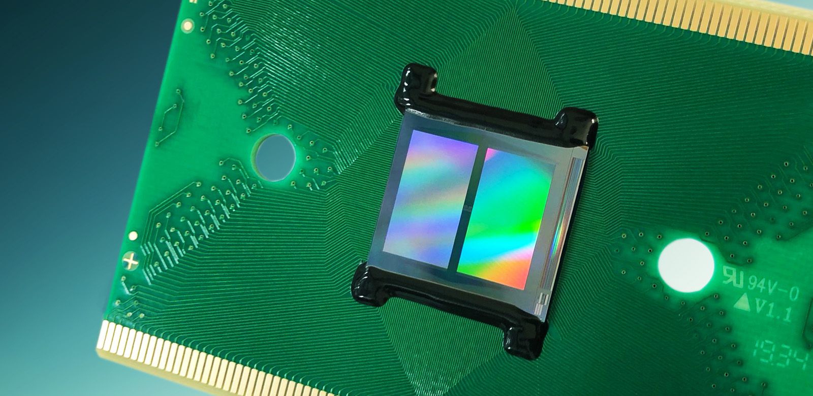
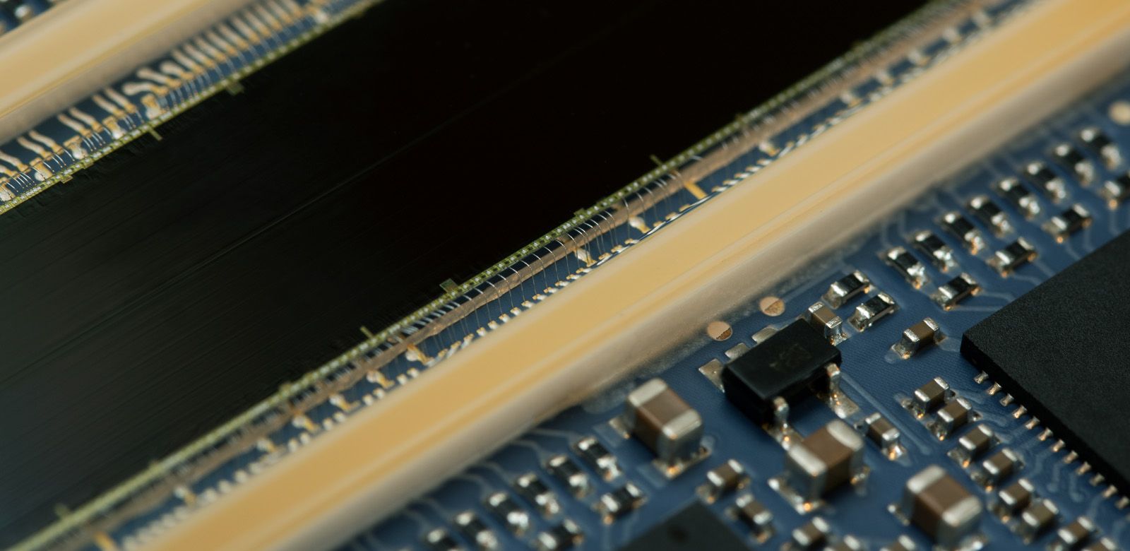
Eurotronics offers a wide range of services in the production of complex substrates in thick-film technology as well as microelectronic (wire bond) assembly on ceramics or conventional PCBs for amongst others research & development, medical and demanding industrial applications.
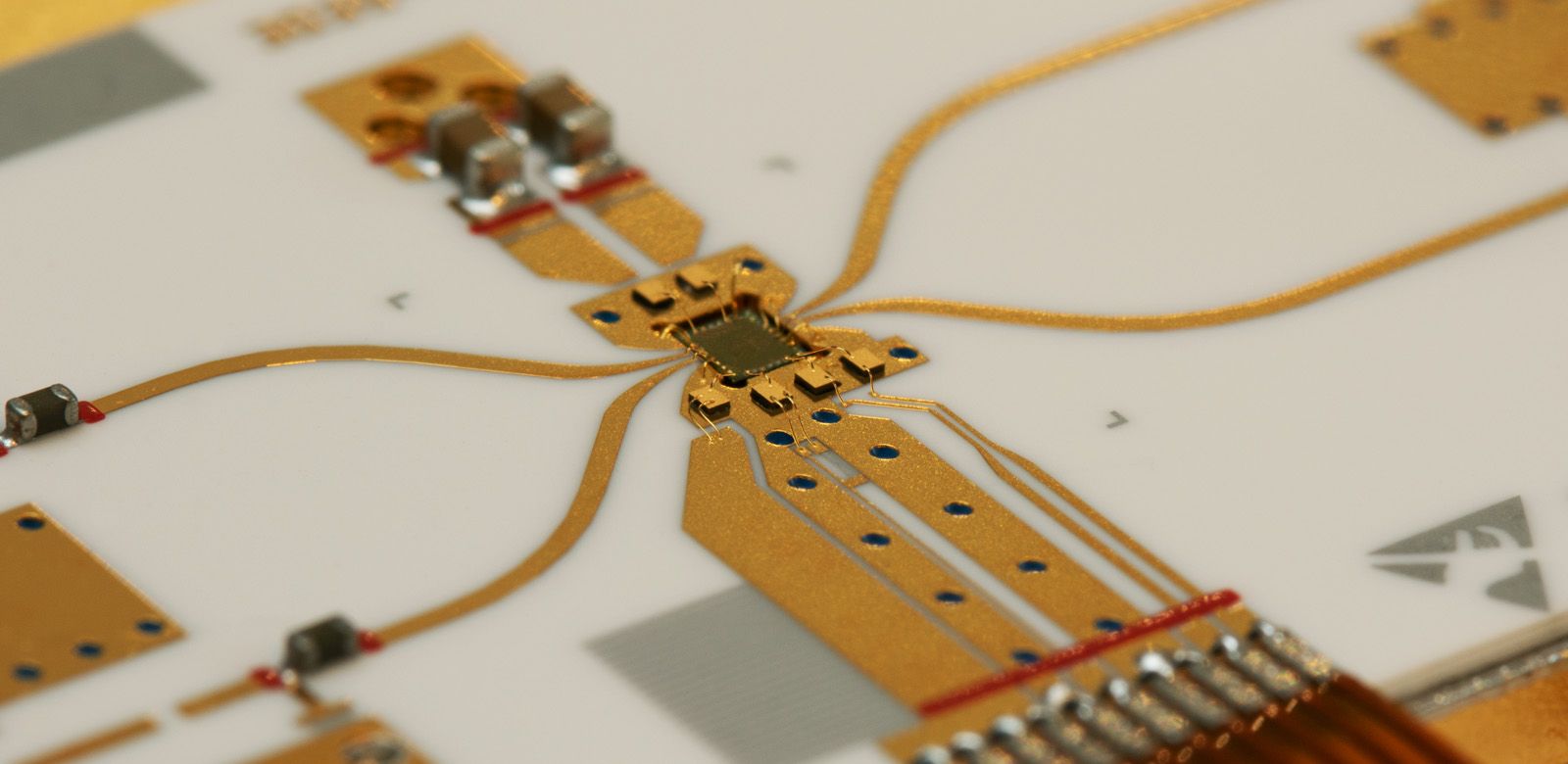
Thick & thin film technology, performed by our partner production facility in Germany, is a highly sophisticated technology for the production of wiring supports that has been in use for decades. The conductor tracks are being applied by screen printing and then burned in. Ceramic substrates provide the advantage of excellent thermal conductivity, mechanical properties and service life.
Printed resistors with a wide spectrum of electrical values from Mega Ohms (mΩ) up to Giga Ohms (gΩ), can be realized directly on the substrate with tight tolerances by means of laser trimming. Active trimming provides the possibility to adjust the electrical output signals of a circuit during operation in real-life scenario.

Specific services
- Feasibility studies
- Qualification of components and products
- Redesign and obsolescence management
- PCB layout
- Support in product development
- Optimization of manufacturing processes
- Development of customer-specific test equipment
- Project management
- Processing of ceramic, steel or glass substrates
- Screen printing of conductive pastes and resistor pastes
- Structure resolution down to 80 μm line/space
- Solderable and bondable surface finishing
- Active and passive resistance adjustment with laser
- Clean rooms up to ISO class 5 (class 100)
- Processing of thick-film substrates and conventional PCBs
- Traceability of all assembled components
- Solder paste inspection (SPI) and component inspection (AOI)
- Assembly of SMD components
- COB or flip chip from wafer or waffle pack
- Reflow soldering and vacuum soldering
- Processing of lead-free and lead-containing solders
- Bonding with insulating and conductive adhesives
- Ball/wedge and wedge/wedge wire bonding 12.5 μm to 500 μm Ribbon bonding
- Glob top and coating
- Hermetic encapsulation
- Flying probe
- Temperature cycling test Moisture test
- Burn-in
- Acceleration and vibration test Leakage
- X-ray
- In-circuit
- Electrical test
- Endurance test

